Deep-Dive Series // 7 Steps

Designing the MonkiiBoard58

How we drew our first wireless keyboard, and why each part is on the board

Difficulty

Advanced

Time

2–3 evenings

Steps

7 stages

Every file for this build is up on GitHub, the plates, the case and the firmware

Our GitHub

Before You Build

Gather everything below before you start and the whole build goes a lot smoother. The printable parts are on GitHub, so you only need to buy the hardware.

Component Manifest

Component Qty Specification
ESP32-S3-WROOM-1 1 The MCU. Bluetooth LE, Wi-Fi and native USB in one module
MX-compatible switches 58 5 rows × 12 columns, two positions left empty for the wide keys
1N4148 diodes 58 One per switch, so held chords do not ghost
USB-C receptacle 1 Charging and flashing
TP4056 charger IC 1 Li-ion charging, with a status LED
Li-ion battery + JST connector 1 Check polarity before you plug it in
AMS1117-3.3 regulator 1 Battery voltage down to a steady 3.3V
AO3401A P-MOSFET 1 Lets the MCU cut power to the OLED
0.91" OLED (SSD1306) 1 Four wires over I²C
EC11 rotary encoder 1 With a push switch

Tools Required

01

KiCad 7 or newer

02

A fab house that accepts Gerbers (JLCPCB, PCBWay, OSH Park)

03

Patience for the matrix section

Build Steps

Work through these in order. Anything you need to download along the way, the plates, the case and the firmware, is already waiting for you on GitHub.

01

Step 1 of 7

Pick the brain first

Everything else follows from the MCU, so start there. We chose the ESP32-S3-WROOM-1 because it does Bluetooth LE, Wi-Fi and native USB with no extra chips, and has plenty of GPIO for a 5×12 matrix, an encoder and a screen. We would suggest the module over a bare chip: it is pre-certified and saves you drawing an RF front end.

Pro Tip

Add a reset circuit early: a push switch to ground, a 10kΩ pull-up to 3V3 and a 100nF cap on the EN pin. It is three parts and it saves a lot of confusion later.
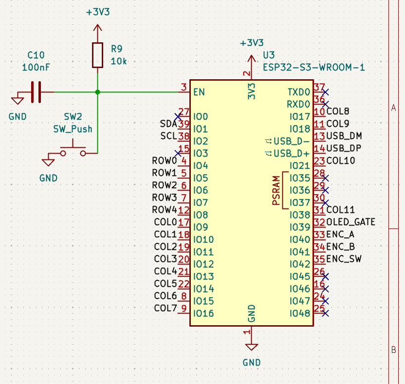
Pick the brain first
Step 1, Pick the brain first

02

Step 2 of 7

Feed it from two directions

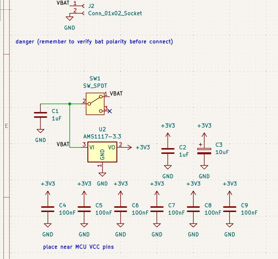
A wireless board runs from a battery and charges over USB, so this section does both. USB-C brings in 5V, a TP4056 charges the cell, an SPDT switch cuts the battery entirely, and an AMS1117 drops it to a steady 3.3V. One detail worth copying: CC1 and CC2 each need their own 5.1kΩ resistor to ground, never a shared one.

Pro Tip

We put 22Ω resistors in series on D+ and D−. They are easy to forget and they keep the USB signal clean.

Feed it from two directions
Step 2, Feed it from two directions

03

Step 3 of 7

Draw the matrix with labels, not wires

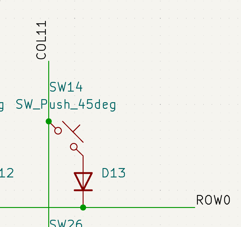
Fifty-eight switches, each with a diode, is the slow part. The trick is net labels: draw one switch-and-diode pair, label the diode ROW0 and the switch COL0, then copy-paste and change the labels. You never drag a wire across the sheet. It is 5 rows by 12 columns, with two positions left empty under the wide keys, which is how 60 becomes 58.

Pro Tip

Diodes all face the same way, cathode to the row. Get one backwards and that key simply never reports.

Draw the matrix with labels, not wires
Step 3, Draw the matrix with labels, not wires

04

Step 4 of 7

Give the screen an off switch

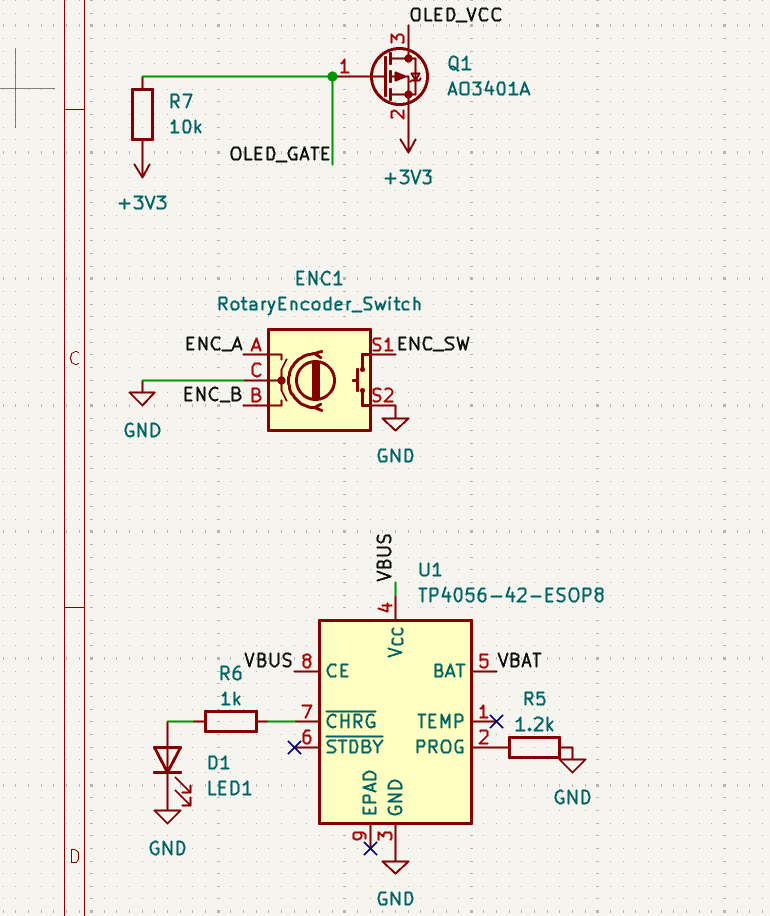
An OLED left running will flatten a battery overnight, so we did not wire it straight to 3.3V. A P-channel MOSFET sits between the rail and the screen, and one GPIO opens that gate, so the firmware can cut the display when the board sleeps. A 10kΩ pull-up keeps it off at power-on. The encoder is simpler: two pins for rotation, one for the push.

Pro Tip

The OLED talks I²C, so it needs 10kΩ pull-ups on SDA and SCL. Without them the screen will look dead even though it is wired correctly.

Give the screen an off switch
Step 4, Give the screen an off switch

05

Step 5 of 7

Import the netlist and meet the pile

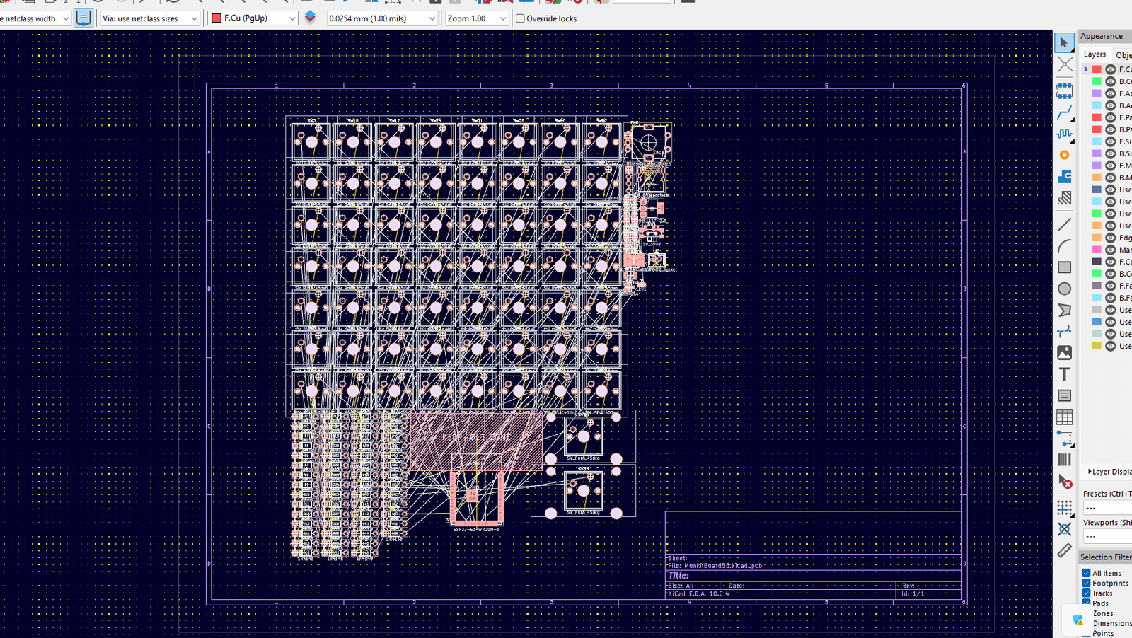
With the schematic done, export the netlist and import it into the PCB editor. Every footprint lands in one heap with thin lines showing what has to connect to what, and nothing is where it belongs yet. This is the least promising a board ever looks, so do not read anything into it. Check the count matches what you drew, then start dragging.

Pro Tip

Set the board outline before you place anything. Knowing the edges makes placing the USB-C connector and the antenna far easier.

Import the netlist and meet the pile
Step 5, Import the netlist and meet the pile

06

Step 6 of 7

Lay it out, and leave the antenna alone

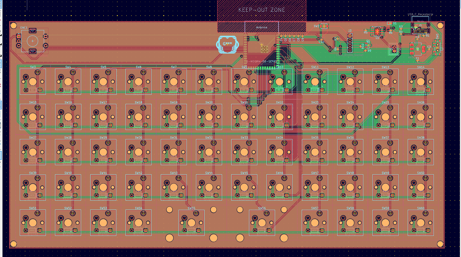
Now place properly: power near the USB-C connector, MCU central, matrix where the keys physically are. The one rule you cannot bend is the module's antenna end, which needs a keep-out with no copper on any layer, no ground pour, nothing underneath. Pour over it and your range drops to almost nothing.

Pro Tip

Hang the antenna end off the edge of the board if you can. It is the easiest way to guarantee the keep-out stays clear.

Lay it out, and leave the antenna alone
Step 6, Lay it out, and leave the antenna alone

07

Step 7 of 7

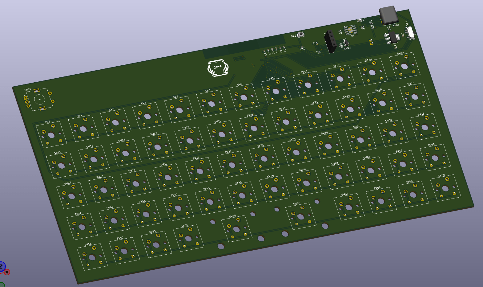
Check everything twice before you spend money

Run ERC on the schematic and DRC on the board, and clear every error rather than filing it away. Most ERC complaints are just missing PWR_FLAG symbols or unused pins wanting a no-connect marker. Then assign footprints, export Gerbers and open them in a viewer before uploading. A fab run costs money and takes weeks, so this is the cheapest twenty minutes of the project. Our output is on GitHub to compare against.

Pro Tip

KiCad's 3D viewer is worth opening at the end. It is the fastest way to catch a connector facing the wrong way.

Check everything twice before you spend money
Step 7, Check everything twice before you spend money

Join the Discussion

Stuck on a step, got a tip, or just finished your build? Drop it in our form. We read every single one and it helps us make the guide better.

Leave a Comment →